
Smart Meter PCB Design for Manufacturability: A DFM Checklist
 Utsav
•
Nov 14, 2026
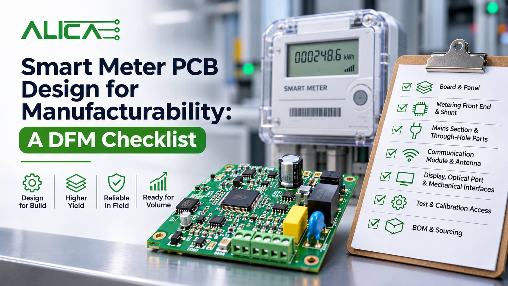
Smart meter programmes run on tight tender schedules, and the board design is usually frozen under pressure. A layout that works on ten hand-built prototypes can still cause trouble at volume: tombstoned passives near the shunt, voids under the metering IC’s thermal pad, through-hole terminals that need hand soldering, or a test fixture that cannot reach the points it needs. Each of these is cheap to fix in the layout file and expensive to fix once thousands of boards are on order. Smart meter PCB design for manufacturability is the review that catches them before release.
This checklist is written for the hardware engineers and NPI leads who release meter boards to a manufacturer. It is not a replacement for the OEM’s product standard or the utility’s specification. It covers the layout, BOM and test decisions that decide how smoothly a meter board moves through SMT, THT, inspection, calibration and box build.
Why smart meter PCB design for manufacturability needs its own review
A meter board is unusual because it puts mains-connected circuits, precision measurement and radio communication in a small space that must last for many years in the field. The OEM designs the meter to its product standard, such as IS 16444 for AC static smart meters in India, and to the utility’s specification. Those documents set the electrical and safety requirements. DFM is about how the design is built, which is a separate question.
Four features make meter boards demanding to manufacture:
- Mixed technology. Fine-pitch SMT parts such as the metering IC and MCU sit next to heavy through-hole parts: terminals, relays, current transformers, large capacitors and MOVs.
- Precision measurement. The shunt or current sensor and its sense lines decide accuracy. Solder joint quality and component tolerance show up directly in calibration results.
- Long field life with little maintenance. Latent joint defects, especially under bottom-terminated parts, become field returns years later.
- High volume on a fixed schedule. Small yield losses multiply across large tender quantities, and rework stations become a bottleneck.
The live guide to smart meter PCB assembly and box build describes the full build from board to finished meter. The checklist below focuses on the decisions the design team controls.
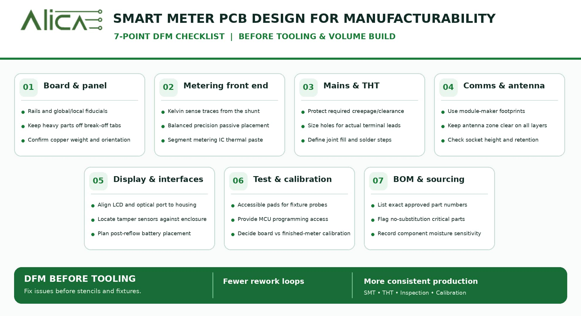
The smart meter DFM checklist, section by section
1. Board and panel
- Panel the board with rails and at least three global fiducials, plus local fiducials near the metering IC and any fine-pitch part.
- Keep heavy through-hole parts away from break-off tabs so depanelling does not stress their joints.
- Choose one panel orientation for SMT and THT so the board does not have to be rotated between processes.
- Confirm the copper weight in the current path with the fabricator early, because heavy copper affects reflow heating.
2. Metering front end and shunt
- Lay out the shunt sense connections as true four-wire (Kelvin) traces taken from the agreed points on the shunt, not from the high-current copper.
- Keep precision passives in the measurement path on the same side and in a consistent orientation, which helps AOI and reduces tombstoning.
- Avoid placing small passives in the shadow of tall through-hole parts, where reflow heating is uneven.
- Define the metering IC’s thermal pad paste pattern as segmented windows, not a single opening, to reduce voids and floating.
3. Mains section and through-hole parts
- Follow the creepage and clearance distances required by your product standard, and mark them on the assembly drawing so the manufacturer does not move parts into the gap during rework.
- Size through-hole pads and holes for the actual lead dimensions of terminals and relays, with thermal relief on large copper pours so joints fill properly.
- Group through-hole parts so they can be soldered in as few steps as possible, and say on the drawing which parts must be hand soldered.
- Specify the solder fillet requirement for terminals and relays, since these carry load current for the life of the meter.
4. Communication module and antenna
- Keep the module footprint exactly to the module maker’s recommended land pattern, including paste reduction under castellated or LGA pads.
- Respect the antenna keep-out on every layer and leave room for the enclosure walls the antenna sees in the finished meter.
- Where the module is socketed or plug-in, define the mating height and retention so box build does not stress the board.
5. Display, optical port and mechanical interfaces
- Check LCD connector and optical port positions against the enclosure model, not only the PCB outline.
- Place tamper switches, magnetic sensors and push buttons where the enclosure features actually land.
- Add the backup battery or supercapacitor after reflow if the part cannot survive the reflow profile, and state this on the drawing.
6. Test and calibration access
- Bring every signal the functional test needs to a test pad on one side of the board, with enough spacing for spring-loaded fixture pins.
- Provide a programming header or pads for the MCU firmware load, reachable while the board sits in the fixture.
- Agree with the manufacturer whether calibration happens at board level or on the finished meter, because that changes which points must stay accessible after box build.
7. BOM and sourcing
- List approved manufacturers and part numbers for every line, and mark which parts have no alternate, such as the metering IC.
- Avoid parts close to end of life for a product that will be built over several years of tenders.
- Note moisture sensitivity levels for the metering IC, MCU and module so storage and baking are planned.
Design decisions and their effect on the build
| Design decision | What goes wrong if it is missed | How it shows up in production |
|---|---|---|
| Single large paste window on the metering IC thermal pad | Excess voiding, part floats off its pads | X-ray rejects, calibration drift |
| Small passives next to tall THT parts | Uneven heating, tombstones and opens | AOI rejects and rework |
| No thermal relief on terminal pads in heavy copper | Poor hole fill on load-carrying joints | Hand rework, risk of field failures |
| Test points under the enclosure or on both sides | Fixture cannot reach them | Slow manual testing or untested nets |
| Antenna keep-out ignored near ground pours | Weak radio performance | Communication failures at final test |
| Parts without approved alternates | Line stops during a shortage | Missed tender delivery dates |
For procurement: what DFM does for cost and supply
Purchase teams benefit from DFM review more than they often realise. A BOM that lists approved alternates, avoids end-of-life parts and flags single-source items is easier to buy during a shortage. Fewer hand-soldered parts and fewer rework steps also mean a lower and more predictable assembly cost. The article on choosing a smart meter contract manufacturer in India covers sourcing and cost transparency in more detail.
For operations: consistent batches and fewer field returns
Plant and quality heads see the result of DFM in yield and in field returns. A board designed for inspection lets SPI, AOI and 3D X-ray do their job, and a board designed for testing lets every unit go through the same functional test and burn-in. The testing and inspection page sets out how each stage works on Alica’s line. For a broader view of what inspection catches, see common PCB assembly defects and how inspection catches them.
How Alica supports smart meter DFM
Alica Technologies carries out early DFM review before tooling, as part of its SMT and THT PCB assembly service. The review looks at pad and paste design, panel layout, through-hole sequencing, test access and BOM risk, and findings go back to the design team before stencils are ordered. Builds then run with inline SPI, AOI, 3D X-ray on hidden joints, functional testing and burn-in, following IPC-recommended procedures with 100% inspection coverage. A similar checklist for battery boards is in the BMS PCB DFM checklist.
Frequently Asked Questions
What is smart meter PCB design for manufacturability?
It is a review of a smart meter board’s layout, BOM and test plan to make sure it can be built reliably at volume. It covers paste and pad design, through-hole parts in the mains section, the shunt and metering front end, communication module footprints, test and calibration access, and component sourcing.
When should a DFM review happen for a smart meter board?
Before the design is released for tooling, ideally after the first prototype build. At that stage changes are still file edits. After stencils, fixtures and volume orders are in place, the same changes cost far more time and money.
Does DFM replace testing to the meter’s product standard?
No. The OEM still designs and type tests the meter to its product standard and the utility’s specification. DFM deals with how the board is built, so that every unit made in production matches the design that passed those tests.
Send your meter board for a DFM review
If your team is preparing a smart meter board for release, Alica can review the files before tooling and build pilot batches from its facility in Changodar, Ahmedabad. See the full list of assembly and test capabilities or get in touch with the Alica team to share your design.
Tagged in
Looking for a reliable EMS partner?
Get a quote for PCB assembly, turnkey manufacturing, or prototype builds.
Get in Touch