
BMS PCB design for manufacturability: A 12-point DFM checklist before you release files
 Utsav
•
Oct 8, 2026
Utsav
•
Oct 8, 2026
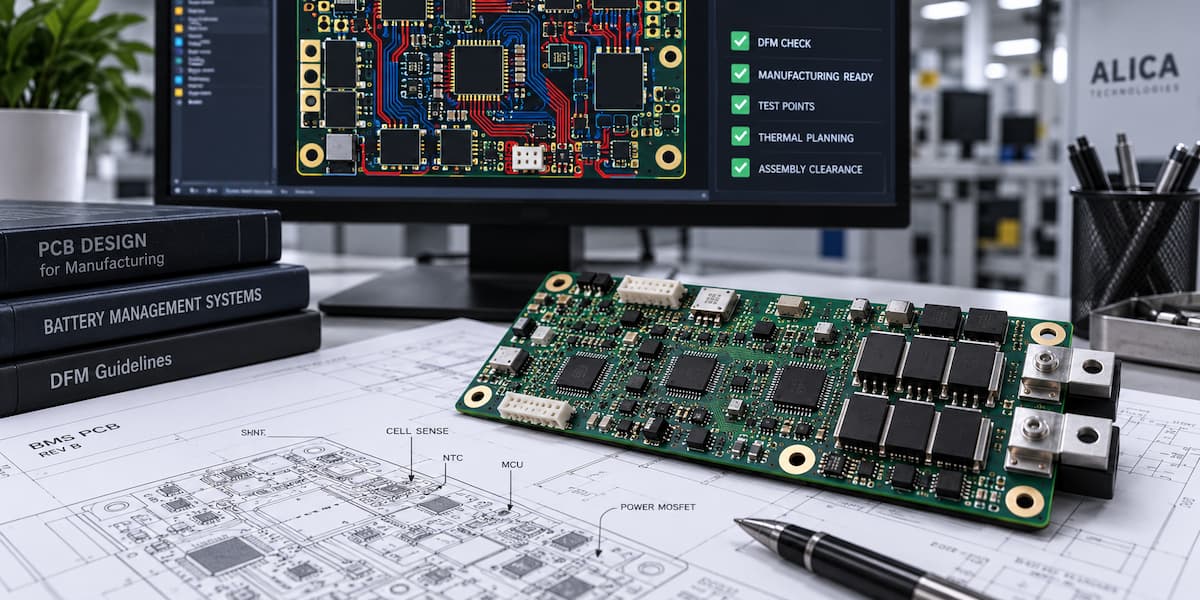
Most BMS revisions are not caused by a bad schematic. They are caused by small layout decisions that make the board hard to build, hard to inspect, or hard to test: a shunt with no clean sense routing, a balancing resistor cooking its neighbours, a QFN pad that traps voids, a connector nobody can reach after assembly. Good BMS PCB design for manufacturability removes those problems before the first board is built.
This checklist is for hardware and embedded engineers about to release BMS files. It pairs with our overview of BMS PCB assembly and battery management system manufacturing and with how Alica builds BMS boards, which shows where each of these points surfaces on our line.
Why DFM matters more on a BMS than on a typical board
A BMS combines precision analog sensing, high-current power paths, fine-pitch ICs, and heavy through-hole parts on one board. Each area has its own manufacturing sensitivities, and they interact. A layout that is electrically correct can still produce inconsistent measurements or hot spots if it is not built the way it was drawn. DFM is how you close that gap, and an SMT and THT assembly partner who reviews files early will catch most issues in a day or two instead of after a failed build.
The 12-Point BMS DFM checklist
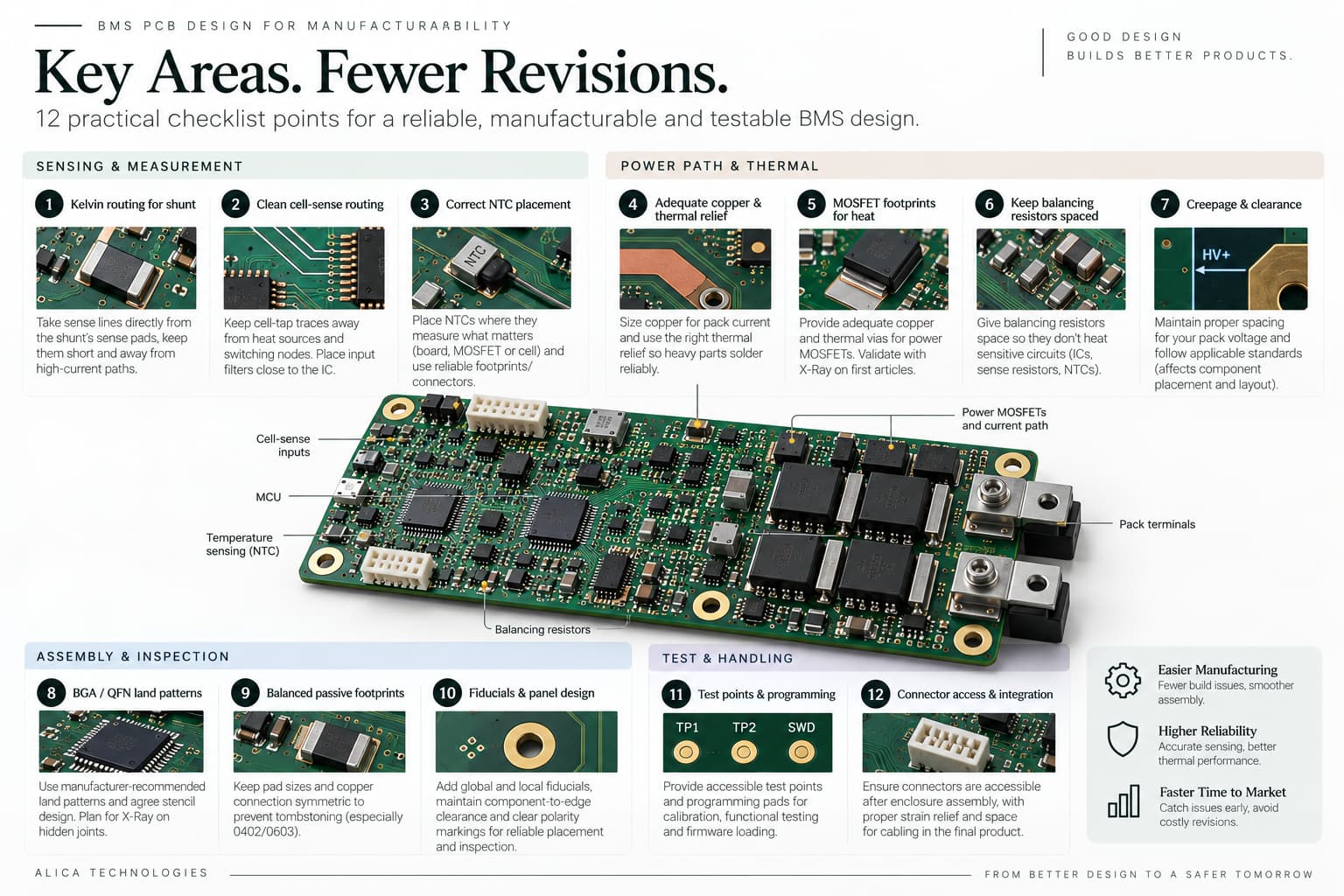
Sensing and Measurement
1. Route shunt sense lines as a proper Kelvin connection
Take sense traces directly from the shunt’s sense pads, not from the high-current copper. Keep the pair tightly routed and away from switching nodes. Check that the shunt footprint gives repeatable solder fillets, since uneven solder on a low-value shunt can shift current readings.
2. Protect cell-sense lines from heat and noise
Cell-tap traces into the monitoring IC should avoid running beside balancing resistors, MOSFETs, or other heat sources. Thermal gradients and coupling both show up as measurement error. Place input filter components close to the IC with consistent orientation so placement and inspection stay predictable.
3. Place NTC thermistors where they measure what matters
Decide early whether an NTC is meant to read board temperature, a MOSFET, or a remote cell, and place or connect it accordingly. Confirm the footprint allows reliable soldering and that wiring for remote sensors has a robust connector, not a bare pad that will be hand-soldered.
Power Path and Thermal
4. Give power paths enough copper and the right thermal relief
High-current traces and pours need adequate width and copper weight for your pack current, but thermal relief on through-hole terminals and large pads also has to let solder wet properly. Over-connected pads can cause cold joints on heavy parts, and under-connected pads can overheat in use. Review these pads specifically with your assembler.
5. Design MOSFET footprints for heat and solderability
Power MOSFET thermal pads need adequate copper and, where appropriate, thermal vias, but via placement under the pad affects solder voiding. Agree the approach with your assembly partner and check the result with X-Ray on first articles.
6. Separate balancing resistors from sensitive circuitry
Passive balancing resistors dissipate heat during balancing. Space them so they do not heat the monitoring IC, sense resistors, or NTCs, and make sure the pad and copper layout can handle the dissipation without lifting or discolouring the board.
7. Respect creepage and clearance for your pack voltage
Spacing between high-voltage nets, between pack terminals, and around connectors should follow the standards that apply to your product and voltage. Confirm these before layout freeze, because they also affect how close components can sit and how the board is handled and coated.
Assembly and Inspection
8. Get BGA and QFN land patterns and stencil apertures right
Use manufacturer-recommended land patterns and agree stencil aperture design with your assembler. Exposed thermal pads on QFNs are a common source of voiding, and this is where inline SPI and X-Ray earn their keep. If there are hidden joints, plan for the board to be inspected, not just powered up.
9. Keep passive footprints balanced to prevent tombstoning
Small 0402 and 0603 parts with unequal pad sizes, unequal copper connection, or one end tied to a large pour can tombstone in reflow. Symmetric pads and matched thermal connection on both ends avoid a defect that AOI will flag but rework will not always fix cleanly.
10. Add fiducials, panel rails and clear polarity marking
Global and local fiducials let the placement machine align accurately, especially for fine-pitch parts. Keep component-to-edge clearance appropriate for the panel and add clear polarity and pin-one markings so AOI programming and manual checks are unambiguous.
Test and Handling
11. Provide test points and programming access
Decide how the board will be flashed, calibrated, and functionally tested, then put test points and programming pads where fixtures can reach them. Late discovery that a fixture cannot reach a signal is a common reason burn-in and functional testing get compromised.
12. Think about connector access and the finished product
Check that connectors can be mated after enclosure integration, that cable strain relief is considered, and that nothing blocks box build assembly. A board that is easy to build but hard to integrate still causes problems on the line.
Quick reference: Who cares about what
| Checklist area | Main risk if missed | Where it shows up |
|---|---|---|
| Shunt and cell sensing (1 to 3) | Measurement error, poor state-of-charge accuracy | Bench calibration, field drift |
| Power path and thermal (4 to 7) | Hot spots, cold joints, lifted pads | Burn-in, field heat failures |
| Assembly and inspection (8 to 10) | Voids, tombstones, misplacement | SPI, AOI, X-Ray |
| Test and handling (11 to 12) | Untestable boards, integration delays | Functional test, box build |
How an early DFM review works at Alica
Our engineers review your Gerbers, BOM, pick-and-place data, and assembly drawings before tooling, looking at footprints, thermal relief, panelization, and placement. Findings come back to you in writing so you can decide what to change, and this sits alongside our 5 to 10 day rapid NPI turnaround so a revised board does not cost you weeks. If you are still deciding on a partner, see how to choose a BMS manufacturer in India for what to ask, and review our testing and inspection methods to see how issues like voiding and hidden joint defects are verified.
Frequently Asked Questions
What is DFM for a BMS PCB?
Laying out the board so it can be assembled, inspected, and tested reliably and repeatably. It covers footprints, thermal design, sense-line and shunt layout, panelization, fiducials, stencil considerations, and test access.
When should I send BMS files for a DFM review?
Before you release the board for fabrication and tooling, once layout is substantially complete. Changes at that stage are cheap; changes after the first build cost time, boards, and sometimes a full revision.
Does Alica review BMS designs before assembly?
Yes. We perform early DFM reviews before tooling and report findings in writing alongside a quote.
Send us your BMS layout before you release it
A short DFM review costs far less than a respin. Send your files through our contact page and we will come back with feedback and a quote, or explore our manufacturing capabilities first.
Tagged in
Looking for a reliable EMS partner?
Get a quote for PCB assembly, turnkey manufacturing, or prototype builds.
Get in Touch