
Medical Device PCB Assembly: Manufacturing for Diagnostics and Monitoring
 Utsav
•
Nov 14, 2026
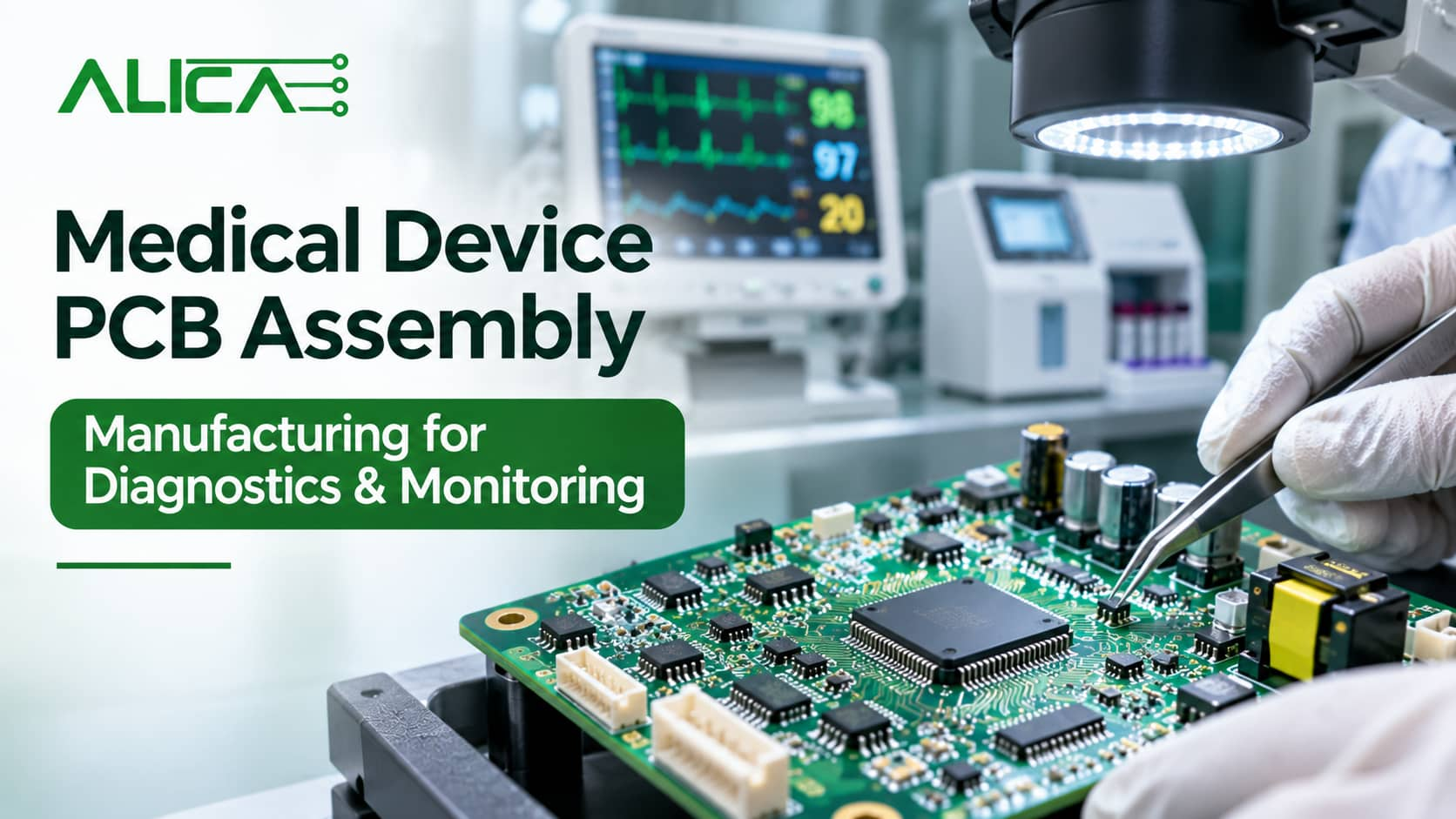
A diagnostic analyser or patient monitor can pass every bench test in the lab and still fail its first pilot batch. A hidden void under a BGA, a QFN that lifts on one corner, a sensor front end that drifts because a passive came from a different lot: these are the faults that turn a planned design freeze into months of delay. For hardware teams building medical products, medical device PCB assembly is where the design meets reality, and the assembly partner decides how much of that reality is found in the factory rather than in a hospital.
The difficulty is that medical OEMs carry the regulatory responsibility for their device, while the board itself is often built by someone else. The R&D team needs a partner that builds exactly to the released design, inspects joints that cannot be seen, records what went into every unit and supports quick prototype turns while the design is still changing. This guide explains what makes medical electronics hard to build and what to agree with an EMS partner before the first order.
Why medical electronics are hard to assemble
Most diagnostic and monitoring products combine three things on one or two dense boards. There is an analogue front end that measures very small signals, such as ECG electrodes, SpO2 photodiodes, temperature sensors or the detector in an analyser. There is a processor, often a fine-pitch BGA or a QFN microcontroller, with memory and a display interface. And there is power and connectivity: a battery charger, isolated supplies for patient-connected parts, and Bluetooth, Wi-Fi or cellular modules.
Each of these brings its own assembly risk. Small analogue signals are sensitive to leakage, contamination and component tolerance, so a solder defect that would be harmless on a consumer gadget can shift a reading. Fine-pitch BGAs and bottom-terminated parts hide their joints, so visual inspection alone cannot confirm them. Portable and wearable devices push components closer together, which leaves little room for rework. And because a device may stay in service for years, latent defects such as cracked joints or marginal wetting matter more than they would in a product that is replaced every year.
There is also the regulatory layer. In India, medical devices are regulated under the Medical Devices Rules, 2017, which place devices in four risk classes, A (low risk) to D (high risk), with Class C and D devices licensed by the Central Licensing Authority (CDSCO). Medical electrical equipment is commonly designed to the IEC 60601-1 family of standards for basic safety and essential performance. These obligations belong to the device manufacturer and its product design. The assembly partner’s job is to build the design faithfully and keep the records the OEM needs to show that it did.
What R&D teams need from medical device PCB assembly
For the hardware lead or NPI manager, the assembly partner is judged on three things: how much of the design risk it catches before production, how well it inspects what it builds, and how quickly it turns prototypes while the design is still moving.
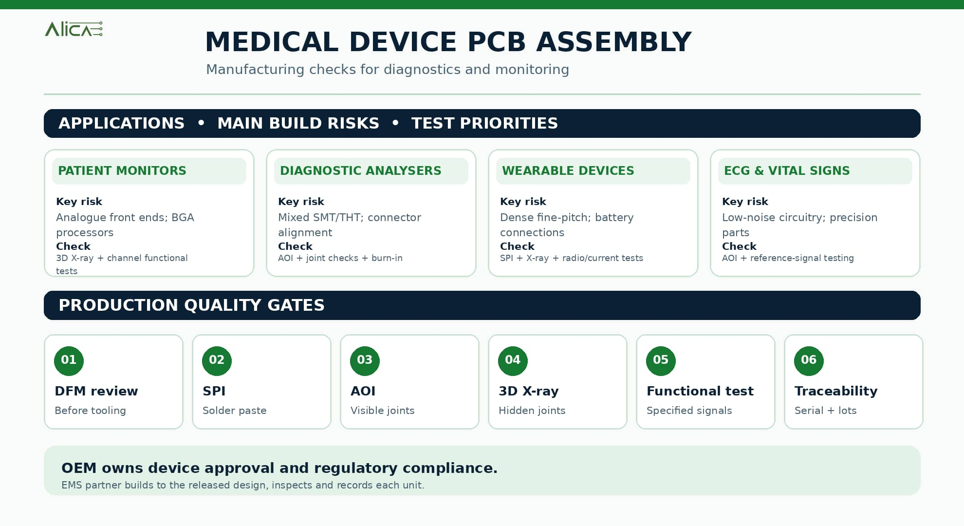
DFM review before tooling
An early design for manufacturability review is the cheapest place to remove defects. For medical boards, the useful checks are pad and paste design for BGAs and QFN thermal pads, spacing around fine-pitch parts, test point access for the functional test fixture, fiducials, panel layout and component choices that are close to end of life. The general principles are covered in the guide to designing PCBs for high-yield assembly. Alica Technologies carries out DFM review before tooling, so issues are raised while they are still a file change rather than a stencil change.
Inspection of joints you cannot see
Inline solder paste inspection checks paste volume and position before components are placed, which matters most on fine-pitch parts where a small paste error becomes a bridge or an open. AOI after reflow checks placement, polarity and visible joints. 3D X-ray is what confirms BGA balls, QFN centre pads and other hidden joints, including voids. The article on common PCB assembly defects and how inspection catches them explains which method finds which fault. Alica runs SPI, AOI and 3D X-ray with 100% inspection coverage, following IPC-recommended procedures.
Mixed technology on one board
Many monitoring devices still need through-hole parts: patient cable connectors, larger power components, battery terminals and mechanically stressed headers. A partner that handles SMT and THT on the same board avoids splitting the build between two suppliers. The trade-offs are covered in the SMT vs THT technical guide, and the line capability is on the SMT and THT PCB assembly page.
Rapid prototyping while the design changes
Medical designs often go through several revisions during verification testing. Each revision needs boards quickly, built on the same process that will be used in production, so test results carry over. Alica offers rapid prototyping and NPI support, which lets hardware teams test changes without waiting weeks for each spin.
Medical electronics manufacturing by device type
Different medical products stress different parts of the build. The table below is a starting point for planning inspection and test focus.
| Device type | Typical board features | Main assembly risk | Inspection and test focus |
|---|---|---|---|
| Patient monitors | Multi-parameter analogue front ends, processor BGA, display, isolated supplies | Hidden joints on the processor, leakage in the front end | 3D X-ray on BGAs, AOI, functional test of each parameter channel |
| Diagnostic analysers | Detector and sensor boards, motor drivers, control boards, many connectors | Mixed SMT and THT, connector joints, board-to-board alignment | AOI, THT joint inspection, functional and burn-in testing |
| Wearable and telemetry patches | Very small, dense boards, micro-BGA or wafer-level parts, BLE module, battery | Fine-pitch placement, little space for rework | SPI, 3D X-ray, current draw and radio checks |
| ECG and vital sign devices | Low-noise amplifiers, precision passives, electrode connectors | Component tolerance, contamination near sensitive nodes | AOI, functional test against reference signals defined by the OEM |
For procurement: sourcing and traceability
Purchase teams face a specific problem with medical products: the approved parts list is hard to change. Once a design has been verified and documented, swapping a component means re-testing and updating the design records, so a shortage is more expensive than it would be for a consumer product. A turnkey partner that manages the full BOM can plan purchases against your build schedule, flag parts at risk early and propose alternates for your engineering team to approve in writing. Alica works on this model with transparent cost breakdowns, described on the turnkey project delivery page.
Component traceability is the other requirement. If a field issue appears, the OEM must be able to identify which component lots and which build went into the affected serial numbers. Ask to see a sample traceability record before the first order.
For operations: from boards to finished units
Plant and operations heads care about batch-to-batch consistency and about how many suppliers touch the product. Functional testing and burn-in testing catch early-life failures in power supplies, batteries and radios before units ship. Where the OEM wants finished products rather than boards, box build brings enclosure assembly, wiring and final test under one roof. The steps are explained in box build assembly from bare PCB to finished product.
Checklist before you place a medical PCB assembly order
- Have you shared the full release package: Gerbers, assembly drawings, BOM with approved manufacturers, and test requirements?
- Has the partner completed a DFM review, and have you closed every finding in writing?
- Which joints will get 3D X-ray, and what void limits will be applied?
- Is SPI run on every board, not just on first articles?
- What exactly does the functional test check, and who provides the fixture and test limits?
- Is burn-in testing needed for your power or battery circuits?
- How are component substitutions proposed and approved?
- Can the partner show a sample serial-level traceability record?
- Which quality system certifications does your regulatory plan require from suppliers, and has the partner confirmed them in writing?
- Who owns the device’s regulatory submissions and product standard testing, and is that written into the agreement?
Frequently Asked Questions
What is medical device PCB assembly?
Medical device PCB assembly is the placement and soldering of components on the circuit boards used in medical products such as patient monitors, diagnostic analysers and wearable health devices. It usually combines fine-pitch SMT, some through-hole parts, inspection of hidden joints with X-ray, functional testing and component traceability.
Is the EMS partner responsible for medical device regulatory approval?
No. The device manufacturer is responsible for regulatory approval and for designing the product to the applicable standards. The EMS partner builds the board to the released design, inspects and tests it as agreed, and keeps the build and traceability records the manufacturer needs.
Why is X-ray inspection important for medical electronics?
Many medical boards use BGAs, QFNs and other parts whose joints sit underneath the component. AOI cannot see these joints. 3D X-ray shows voids, bridges and opens under the part, so hidden defects are found in the factory rather than in the field.
Talk to Alica about your medical electronics build
Alica Technologies builds PCB assemblies and box build products from its facility in Changodar, Ahmedabad, with SPI, AOI, 3D X-ray, functional testing and full BOM management. To discuss a diagnostic or monitoring product, review the manufacturing capabilities or contact the Alica team with your design files.
Tagged in
Looking for a reliable EMS partner?
Get a quote for PCB assembly, turnkey manufacturing, or prototype builds.
Get in Touch