
Common PCB Assembly Defects and How Inspection Catches Them
 Utsav
•
Nov 11, 2026

A board can pass a quick visual check and still fail in the field a few months later. Most PCB assembly defects start as small process variations: slightly too much solder paste, a part sitting a fraction off its pads, a void hidden under a BGA ball. On one board they look minor. Across a production batch they turn into returns, rework and lost confidence.
This guide covers the defects that come up most often, why they happen, and which inspection step is best placed to catch each one. It is written for the engineers and plant teams who decide how much inspection a product really needs.
Where defects come from in the assembly process
Surface-mount assembly runs in a fixed order. Solder paste is printed onto the pads through a stencil, components are placed on the paste, and the board passes through a reflow oven that melts the solder. Through-hole parts are soldered in a separate step. Each stage has its own failure modes, and a fault caught early is far cheaper to fix than one found after reflow. Many soldering defects trace back to the paste printing step, which is why paste inspection sits at the very start of a well-run line.
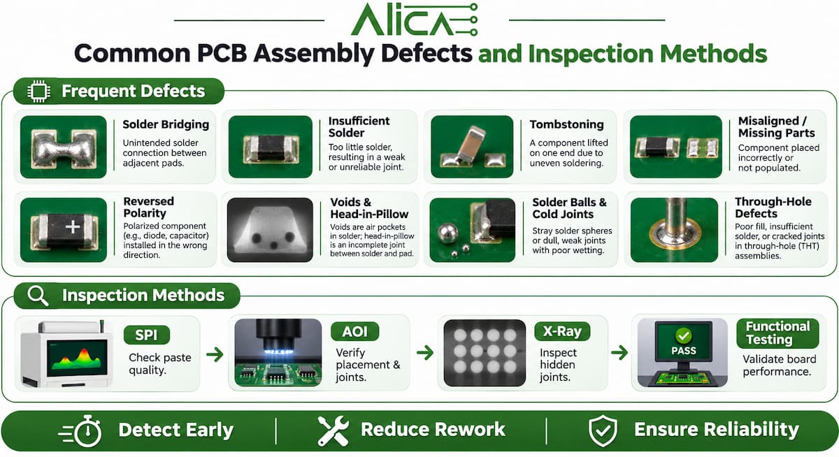
The most common PCB assembly defects
Solder bridging
Excess solder joins two neighbouring pins or pads and creates a short circuit. It is most common on fine-pitch ICs and connectors. Typical causes are too much paste, stencil apertures that are too large, a misaligned print, or placement pressure squeezing paste sideways.
Insufficient solder and open joints
Too little solder leaves a weak joint, or no electrical connection at all. Blocked stencil apertures, poor paste release and component leads that do not sit flat on their pads are the usual causes.
Tombstoning
A small chip resistor or capacitor lifts at one end and stands upright during reflow, because the solder on one pad melts and pulls before the other. Unequal pad sizes, uneven copper around the pads, uneven paste and placement offset all make it more likely.
Misaligned, missing or wrong components
Parts can be shifted off their pads, rotated, left out, or placed from the wrong reel. These usually come from feeder problems, a wrong reel loaded on the machine, or an error in the placement programme.
Reversed polarity
Diodes, electrolytic capacitors and ICs fitted the wrong way round may pass a glance but will fail in use. Clear polarity marks on the silkscreen and consistent footprint orientation reduce the risk.
Voids and head-in-pillow joints under BGAs
Voids are pockets of gas trapped inside a solder joint. Head-in-pillow is a BGA ball that rests on the paste without fully merging with it, which can pass an electrical test and then fail under heat or vibration. Both are hidden under the package. Reflow profile, paste chemistry, board warpage and oxidised balls are the usual causes.
Solder balls and cold joints
Small spheres of solder scattered across the board can move and cause shorts later. Cold joints look dull and grainy, are mechanically weak, and usually come from too little heat during soldering.
Through-hole joint defects
Through-hole joints can show incomplete hole fill, voids in the barrel or excess solder on the lead. These matter most on connectors and power components that carry current or take mechanical load.
Which inspection catches which defect
| Defect | Best caught by | Why |
|---|---|---|
| Solder bridging | SPI, then AOI | Excess paste is visible before placement; bridges on exposed leads are visible after reflow |
| Insufficient solder, open joints | SPI, AOI, X-ray for hidden joints | Low paste volume shows at print; visible joints after reflow; hidden ones need X-ray |
| Tombstoning | AOI | A component standing on end is easy for a camera to see |
| Misaligned or missing parts | AOI | Each board is compared with the expected position of every part |
| Wrong component value | Functional or electrical testing | Two parts can look identical but have different values |
| Reversed polarity | AOI, functional testing | Polarity marks are checked optically; the board’s behaviour confirms it |
| BGA voids, head-in-pillow | X-ray | The joints sit under the package, out of a camera’s view |
| Cold or intermittent joints | Functional testing, burn-in | Weak joints may only fail under power, heat or time |
The inspection steps explained
Solder paste inspection (SPI) measures the volume, height and area of every paste deposit in 3D before any parts are placed. A bad print found here costs almost nothing: the board is cleaned and reprinted.
Automated optical inspection (AOI) uses cameras to compare each assembled board with a reference. It checks that every part is present, in the right place, the right way round, and that the visible solder joints look correct.
X-ray inspection sees through component packages to the joints underneath. It is the only practical way to check BGA, QFN and other hidden joints for voids, bridges and incomplete wetting.
Functional testing powers the board and checks that it behaves as designed. It catches what no visual method can, such as a wrong-value part or a damaged component. The testing and inspection services page sets out how these steps fit together.
IPC-A-610 and acceptance classes
IPC-A-610 is the widely used industry standard for the acceptability of electronic assemblies. It defines three product classes: Class 1 for general electronics, Class 2 for dedicated service electronics, and Class 3 for high-performance products where downtime is not acceptable. The class decides how strict the accept and reject criteria are, so agree it with your manufacturer before production starts. It affects both the inspection criteria and the cost.
For R&D teams: designing defects out
Many assembly defects are fixed most cheaply on the layout, before a stencil is cut. A layout designed for high-yield assembly avoids most of the common causes. A structured review, such as this 12-point DFM checklist for BMS boards, shows the kind of points worth checking on any product:
- Pad sizes that match the component datasheet, with balanced copper on both pads of small chip parts
- Solder mask between fine-pitch pads to stop bridges forming
- Clear polarity and pin-one markings on the silkscreen
- Fiducials for accurate placement, and test points for electrical testing
- Enough clearance around BGAs and tall parts for inspection and rework
For operations: a defect-prevention checklist
- Agree the IPC-A-610 class for the product before the first build
- Run solder paste inspection on every board, not a sample
- Run AOI after reflow on every board
- Use X-ray for BGA, QFN and other hidden joints
- Complete a first-article inspection on each new build or revision
- Run functional testing, and burn-in where field reliability matters
- Record defects by type, so recurring causes are fixed at the source
- Keep component traceability, so a problem can be traced to a batch
For procurement: what to ask a manufacturer
Inspection is one of the easiest places for two quotes to differ without saying so. Ask each manufacturer which inspections run on every board and which only on samples, whether X-ray is available in-house, and how defects are recorded and reported back. The answers say more about likely field returns than the unit price does, and they belong in any checklist for choosing a PCB assembly partner.
How Alica Technologies inspects its builds
Alica Technologies, an EMS company in Changodar, Ahmedabad, inspects SMT and THT PCB assembly with 3D solder paste inspection, AOI and 2.5D/3D X-ray, with functional testing available. Its processes follow IPC-recommended procedures, and it offers 100% inspection coverage, so every board is checked rather than a sample.
Frequently Asked Questions
What are the most common PCB assembly defects?
The ones seen most often are solder bridging, insufficient solder and open joints, tombstoning, misaligned or missing components, reversed polarity, and voids or head-in-pillow joints under BGA packages.
Can AOI find solder defects under a BGA?
No. The solder joints of a BGA sit underneath the package, where a camera cannot see them. Voids, bridges and head-in-pillow joints under BGA and QFN packages need X-ray inspection.
What is the difference between SPI and AOI?
Solder paste inspection (SPI) measures the printed paste before any components are placed, so print problems can be fixed by cleaning and reprinting the board. Automated optical inspection (AOI) checks the board after placement and reflow, looking at component presence, position, polarity and the visible solder joints.
Talk to an inspection-led EMS partner
To discuss the inspection and testing your product needs, send your board details through the Alica Technologies contact page, or see the full list of manufacturing capabilities.
Tagged in
Looking for a reliable EMS partner?
Get a quote for PCB assembly, turnkey manufacturing, or prototype builds.
Get in Touch