
GPS, GNSS and Satellite Module PCB Assembly: A Guide for OEMs
 Utsav
•
Nov 13, 2026
A GPS tracker that loses its fix inside a warehouse, a fleet unit that reports a position tens of metres off, a timing receiver that drifts after a few weeks in a hot cabinet. When engineers dig into these failures, the cause is often not the firmware or the antenna choice. It sits in the assembly: a shield can that was soldered with a gap, a ground pad under a module with voids, a matching network built with the wrong tolerance part. Satellite module PCB assembly looks simple on a schematic, because the receiver is usually a single module, but the signal it has to pull out of the noise is extremely weak.
For a hardware team, that creates a frustrating gap between the evaluation kit, which works on the bench, and the first production batch, which sometimes does not. This guide explains why GNSS boards are harder to build than they look, what the R&D lead should settle before releasing files, and what procurement and operations teams should check with their manufacturing partner.
Why GNSS boards are harder to build than they look
Satellite navigation signals arrive at the antenna far below the thermal noise floor. The receiver recovers them through correlation, which works only if the front end adds as little noise and loss as possible. Every small assembly variation between the antenna and the low noise amplifier shows up as lost sensitivity, longer time to first fix or a weaker position in difficult conditions.
RF paths are sensitive to small changes
The trace from the antenna feed to the module is usually a controlled impedance line with a small matching network. A solder fillet that is too large on a 0402 or 0201 matching part, a misaligned component or a substituted part with a different tolerance can shift the match enough to cost sensitivity. These defects rarely fail a simple power-on test, so they reach the field unless the line is inspected properly.
Hidden joints under modules and shields
Most GNSS modules are LGA or castellated packages, and many products add a GNSS receiver chip in a QFN or BGA package. The ground pad under these parts carries both the RF ground and heat. Large voids or open joints under a module are invisible to a visual check. Shield cans hide even more of the board once they are placed.
Multi-constellation and multi-band designs
Modern receivers track several constellations at once, such as GPS, GLONASS, Galileo, BeiDou and India’s NavIC, and many now use two frequency bands. That adds filters, diplexers and sometimes a second antenna path. More RF parts mean more places for assembly variation to creep in.
Interference from the rest of the product
A GNSS receiver rarely lives alone. Trackers combine it with a cellular modem, cameras pair it with a video processor and fleet units add CAN or RS-485 interfaces. Switching regulators and digital clocks create harmonics that can land in the GNSS bands. Layout and shielding decide most of this, but poor shield soldering or missing ground stitching on the build can undo good design work.
Satellite module PCB assembly: what the R&D lead should settle first
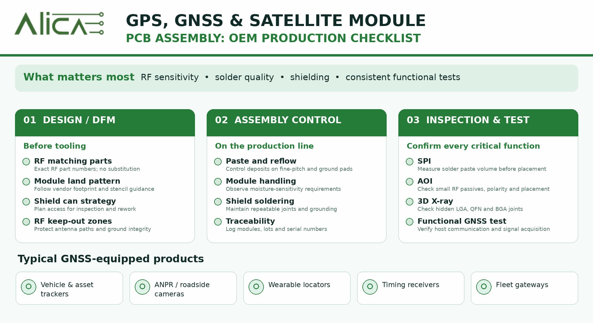
Most problems that show up in a GNSS production batch can be traced back to decisions made, or not made, before files were released. A short design for manufacturability (DFM) review with the assembly partner is the cheapest place to catch them. Alica Technologies offers early DFM review before tooling, which is exactly where these points belong.
- Module footprint and paste aperture. Use the module maker’s recommended land pattern and stencil guidance for the centre ground pad. A window-pane aperture usually controls voiding better than one large opening.
- Shield can strategy. Decide between a one-piece can and a frame with a removable lid. A frame and lid allows inspection and rework of the parts underneath; a one-piece can is cheaper but blocks access.
- Keep-out zones. Mark antenna and RF keep-outs clearly in the fabrication notes so that no test points, labels or mechanical fixings end up in them.
- Matching network parts. Specify exact part numbers and tolerances for RF passives in the BOM, and mark them “no substitution” so a sourcing team does not swap them for a cheaper equivalent.
- Test access. Bring out a test point or connector for the RF path or the module’s serial output so the line can run a functional check without opening the enclosure.
Teams building the GNSS board for a CCTV or ANPR camera can find more on the video side of the product in the guide to choosing a contract manufacturer for IP camera boards. GNSS receivers in vehicles face many of the same thermal and vibration stresses covered in the article on automotive PCB assembly for cars.
Where GNSS modules show up, and what each build needs
The receiver is the same idea in every product, but the assembly priorities change with the application. The table below summarises the common product types in the surveillance, security and telematics space.
| Product | Typical board content | Main assembly risk | Inspection and test focus |
|---|---|---|---|
| Vehicle and asset trackers | GNSS module, cellular modem, MCU, power input stage | Shield soldering, module ground voids, vibration on heavy parts | X-ray of module and modem pads, functional fix test, current draw |
| ANPR and roadside cameras | Video SoC, GNSS for time and location tagging, Ethernet | Fine-pitch BGA on the SoC, heat near the receiver | X-ray of BGA, AOI of RF passives, burn-in |
| Personal safety and wearable locators | Small GNSS module, battery charger, Bluetooth or cellular | Very small passives, tight spacing, battery connections | SPI and AOI on 0201 parts, charge and fix tests |
| Timing receivers for telecom and grid equipment | GNSS timing module, oscillator, PPS output circuitry | Oscillator placement and soldering, clean ground | Functional check of PPS output, thermal soak |
| Fleet and telematics gateways | GNSS, cellular, CAN and RS-485, through-hole connectors | Mixed SMT and THT, connector joint strength | AOI, X-ray, connector pull and functional test |
How inspection protects GNSS sensitivity
Because most GNSS assembly defects do not cause an obvious failure, inspection has to find them before functional test. Alica’s line uses inline solder paste inspection (SPI) to check paste volume on module pads and fine-pitch parts before placement, automated optical inspection (AOI) to check placement and fillets on the RF passives, and 3D X-ray inspection for the joints that cannot be seen: module ground pads, QFN receivers, BGAs and parts under shield frames. More detail on each method is on the testing and inspection services page, which also explains which defect each step is designed to catch.
Functional testing closes the loop. For GNSS products, a practical production test checks that the module powers up, talks to the host, reports the expected firmware version and acquires signals from a simulator or a re-radiated live sky signal within a set time. Burn-in testing is useful for trackers and timing receivers that will run for years in sealed enclosures.
For procurement: sourcing GNSS modules and RF parts
GNSS modules and receiver chips come from a small number of makers, and specific variants can go on allocation with little warning. Procurement teams should ask their manufacturing partner how it handles three things: approved alternates, which should be agreed in advance with R&D rather than chosen on the day; moisture sensitivity, since many modules need baking or dry storage once opened; and lot traceability, so a field issue can be traced back to a module batch. Alica works on a turnkey sourcing model with full BOM management and component traceability, which keeps those records in one place. Teams weighing sourcing models can read about turnkey project delivery.
For operations: keeping batch quality consistent
Plant and operations heads care about whether batch 10 behaves like batch 1. For GNSS products, that means fixed stencil and reflow profiles for the module, a written rule for how shield cans are placed and inspected, and functional test limits that are logged per serial number. Alica follows IPC-recommended procedures on the line and offers SMT and THT PCB assembly on the same board, which suits trackers and gateways that combine fine-pitch RF parts with through-hole power and data connectors. Box build and mechanical assembly can follow on the same project when the product needs to ship as a finished unit.
Checklist before you release a GNSS board for production
- Module footprint and stencil aperture match the module maker’s guidance.
- RF matching parts are listed with exact part numbers and marked “no substitution”.
- Antenna and RF keep-out zones are marked in the fabrication drawing.
- Shield can type (one piece or frame and lid) is agreed with the assembler.
- X-ray inspection is specified for the module ground pad, QFN and BGA parts.
- A functional test plan covers power-up, host communication and signal acquisition.
- Approved alternates for the module and key RF parts are agreed in writing.
- Moisture sensitivity handling for modules is confirmed with the line.
- Lot traceability links each serial number to its module batch.
- Any product certification the device needs is owned and planned by the OEM.
For the wider picture of building security and surveillance products in India, see the buyer’s guide to surveillance and security electronics manufacturing.
Frequently Asked Questions
What is satellite module PCB assembly?
Satellite module PCB assembly is the process of mounting a GPS or GNSS receiver module, its antenna path and supporting circuits onto a printed circuit board, then inspecting and testing the board so that the receiver keeps its full sensitivity in the finished product.
Why do GNSS boards need X-ray inspection?
GNSS modules and receiver chips use LGA, QFN or BGA packages with ground pads that cannot be seen after soldering. X-ray inspection shows voids and open joints under these parts and under shield frames, which affect both RF performance and heat transfer.
Can one board carry both the GNSS module and a cellular modem?
Yes, most trackers and telematics units do this. It needs careful layout, shielding and filtering to keep modem and digital noise out of the GNSS bands, and the assembler must solder shield cans and ground pads consistently so the design works as intended.
Build your GNSS product with Alica Technologies
Alica Technologies builds GNSS, tracker and telematics boards from its facility in Changodar, Ahmedabad, with early DFM review, inline SPI, AOI, 3D X-ray inspection and functional testing. Share your Gerbers, BOM and test requirements through the contact page, or review the full list of manufacturing capabilities first.
Looking for a reliable EMS partner?
Get a quote for PCB assembly, turnkey manufacturing, or prototype builds.
Get in Touch