
IoT Gateway PCB Assembly: Manufacturing Connected Hardware
 Utsav
•
Nov 20, 2026
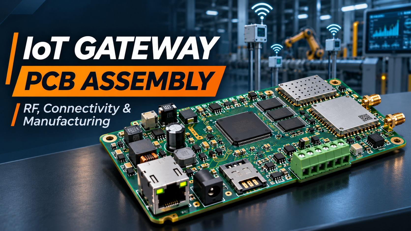
An IoT gateway sits between dozens or hundreds of field devices and the cloud. It collects data over radio links such as Wi-Fi, Bluetooth, LoRa, Zigbee or sub-GHz mesh, then pushes it upstream over Ethernet or a cellular modem. If the gateway drops off the network, every sensor behind it goes quiet too. For hardware teams, IoT gateway PCB assembly is where a design that worked on the bench either becomes a gateway that stays online for years, or a product with weak radio performance, intermittent resets and field returns that are hard to trace.
The difficulty is that a gateway is a small computer, a radio product and a power product on one board. It carries a processor, memory, several radios, antennas or antenna connectors, power conversion and often field wiring. Each of these brings its own assembly risks, and most gateways are built in moderate volumes with several variants for different regions and networks. This guide explains what makes gateway boards hard to build, what R&D teams should settle with their assembly partner, and how purchasing and operations teams fit in.
Why IoT gateway PCB assembly is hard
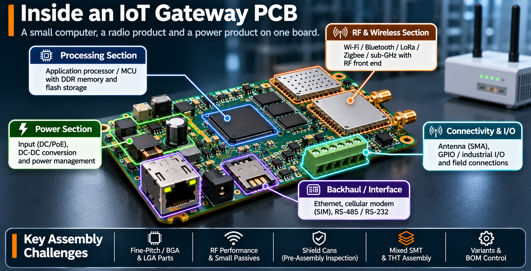
Most gateways follow a similar architecture. There is an application processor or a capable microcontroller, with DDR memory and eMMC or flash storage. There are one or more radio sections, either as certified modules or as chip-down designs with RF front ends. There is a backhaul interface, usually Ethernet, a cellular modem or both. And there is a power stage that may take mains, a DC adapter, Power over Ethernet or a battery.
That combination stresses the assembly process in several ways:
- Fine-pitch and bottom-terminated parts. Processors and memory often come in BGA packages, and many radio and power ICs are QFN or LGA parts. Their joints are hidden under the body, so visual inspection alone cannot confirm them.
- Castellated and LGA wireless modules. Cellular and Wi-Fi modules are large, flat parts with many pads. Paste volume, flatness and reflow profile all affect whether every pad wets properly and whether the module lifts at one corner.
- RF sensitivity. Matching networks use very small passives, often 0201 or 0402, placed close to the radio. A tombstoned or shifted part can detune the radio without causing an obvious failure on a simple power-up test.
- Shield cans. Many radio sections sit under a shield. Once the can is fitted, the parts underneath cannot be seen, so they must be inspected before it goes on, or the can must be a two-piece frame and lid.
- Mixed technology. RJ45 jacks, SIM holders, DC jacks, terminal blocks and SMA connectors are often through-hole or need extra mechanical strength, so the board usually needs both SMT and THT work.
- Variants. The same base board may ship with different radios, modem bands or memory sizes, which means careful BOM control and labelling on the line.
The product itself also carries regulatory work. Wireless products sold in India generally need Equipment Type Approval from the WPC wing of the Department of Telecommunications, and many telecom products, including some IoT gateways, fall under TEC’s Mandatory Testing and Certification of Telecommunication Equipment (MTCTE) scheme. These are the OEM’s product approvals. The assembly partner’s job is to build every unit exactly like the units that were tested.
What R&D teams should agree with an IoT gateway manufacturing partner
Gateway problems that reach the field usually begin as small decisions that nobody settled before the first build. These are the points worth agreeing with the assembly partner early.
Module or chip-down radio
A pre-certified radio module simplifies regulatory work and is easier to assemble consistently, but it costs more and takes more board area. A chip-down design saves cost at volume and gives more control, but it brings fine-pitch RF parts and tighter placement tolerances. Either works. The assembly partner should review the footprint, paste openings and keep-out areas for the option you choose, ideally in a DFM review before the board is released for fabrication.
Stencil and paste for large modules
Large LGA modules and thermal pads under QFNs need controlled paste volume. Too much paste causes bridging and floating; too little leaves open or weak joints. Stencil apertures are often reduced or segmented for these pads. Inline solder paste inspection (SPI) measures the paste deposit on every board before placement, which is the most reliable way to keep these joints consistent across a batch.
Inspection under BGAs and modules
Automated optical inspection (AOI) checks polarity, presence, offset and visible solder fillets on small passives and leaded parts. For BGA processors, memory and bottom-terminated modules, 3D X-ray inspection is needed to see voids, bridges and opens under the package. Agree which parts get X-ray on every board and which are sampled, and make sure shielded areas are inspected before the can is fitted. The testing and inspection process should be written into the build documents, not left to the line.
Programming and functional test
A gateway is not finished when it powers up. Boot loaders, firmware and unique identifiers such as MAC addresses or device certificates need to be loaded, and each radio should be checked to show it can transmit and receive. Decide early who supplies the firmware images and keys, how they are protected, and what the functional test must prove: Ethernet link, cellular registration, radio communication with a reference node, LED and button checks, and power input range. If the product will be deployed outdoors or in hot cabinets, agree whether burn-in is needed and for how long.
Antenna and enclosure integration
Many gateways ship as finished units with internal antennas, cables and an enclosure. Antenna cable routing, connector mating and the position of the board inside the housing all affect radio range. If the assembly partner also handles box build assembly of the finished unit, they can follow a fixed assembly sequence and test the complete product rather than just the bare board.
What procurement teams should check
Gateway BOMs depend on a small number of high-value parts: the processor, memory, cellular modem and radio modules. Lead times on these can change quickly, and a substitute is rarely a drop-in replacement because firmware, certification or footprint may be affected. Procurement teams should ask the partner how they source these parts, how they flag allocation risk early, and how alternates are proposed and approved. A partner offering turnkey sourcing and BOM management should give a transparent cost breakdown so the buyer can see which lines drive the price. Domestic assembly in India also removes one import step for the finished product, which can simplify logistics for gateways sold to Indian utilities, smart city projects and industrial users.
What operations teams should check
For operations and plant teams buying finished gateways, consistency matters more than any single test. Ask how the partner controls firmware versions on the line, how serial numbers link to test results, and how failed units are analysed and reworked. Every shipped unit should have a record of its build lot, inspection results and functional test outcome, so a field problem can be traced back to a batch. Agree on packaging and labelling for units that go straight to site, including any SIM, regional variant or network band markings.
Common gateway types and their assembly focus
| Gateway type | Typical radios and backhaul | Main assembly focus |
|---|---|---|
| Smart metering and AMI gateway | RF mesh or sub-GHz radio, cellular backhaul | LGA modem module joints, mains power section, long field life |
| Industrial IoT gateway | Wi-Fi, Bluetooth, RS-485, Ethernet, cellular | Mixed SMT and THT, terminal blocks, burn-in for cabinet temperatures |
| LoRaWAN gateway | LoRa concentrator, Ethernet or cellular, GNSS for timing | RF front end placement, shield cans, antenna connector strength |
| Building and home automation hub | Zigbee, Thread, Bluetooth, Wi-Fi | Fine-pitch passives in matching networks, cost control at volume |
| Vehicle and asset tracking gateway | Cellular, GNSS, Bluetooth | BGA and module X-ray, vibration-resistant connectors, power input protection |
Some of these overlap with products Alica already covers in depth, such as the smart meter PCB assembly and box build guide and the article on GPS and GNSS satellite module PCB assembly.
IoT gateway build checklist
Use this list before sending a gateway design for quotation or a first build:
- Is the radio a pre-certified module or a chip-down design, and has the footprint been reviewed for DFM?
- Are stencil apertures for LGA modules and QFN thermal pads defined, and will SPI check every board?
- Which parts need 3D X-ray on every unit, and which can be sampled?
- Are shielded areas inspected before the shield can is fitted?
- Who supplies firmware, keys and unique IDs, and how are they loaded and logged?
- What must the functional test prove for each radio, the backhaul and the power input?
- Is burn-in needed for outdoor or cabinet installations?
- Which processor, memory, modem and module lines carry the highest sourcing risk, and what alternates are approved?
- Will the partner deliver bare boards or finished, labelled and packed units?
- Do production units match the configuration used for WPC, MTCTE or other approvals?
How Alica approaches IoT gateway builds
Alica Technologies builds connected hardware from its facility in Changodar, Ahmedabad. The SMT and THT PCB assembly lines handle high-density multi-layer boards with fine-pitch BGAs and modules alongside through-hole connectors on the same board. Every build is checked with inline SPI, AOI and 3D X-ray inspection, following IPC-recommended procedures, and can go on to functional testing, burn-in and box build. Turnkey sourcing, BOM management and component traceability are handled by the same team, so the OEM deals with one partner from components to finished, tested gateway.
Frequently Asked Questions
What is IoT gateway PCB assembly?
IoT gateway PCB assembly is the manufacture of the circuit boards inside gateways that connect field devices to the cloud. It usually involves fine-pitch SMT for processors, memory and radio modules, through-hole connectors for power and Ethernet, X-ray inspection of hidden joints, firmware loading and functional testing of every radio.
Should a gateway use a pre-certified radio module or a chip-down design?
A pre-certified module simplifies regulatory approval and is easier to assemble consistently, while a chip-down design lowers cost at volume but needs tighter RF layout and placement control. Many OEMs start with modules and move to chip-down once volumes justify it. Both should go through a DFM review before release.
Is the assembly partner responsible for WPC or MTCTE approval?
No. The OEM obtains the product approvals its gateway needs, such as WPC Equipment Type Approval or MTCTE certification. The assembly partner builds every unit to the approved design and bill of materials, inspects and tests it as agreed, and keeps build records so production units match the tested units.
Plan your IoT gateway build with Alica
If you are moving a gateway from prototype to production, or looking for a partner that can take it from components to a finished unit, Alica Technologies can review your design and BOM. See the full list of electronics manufacturing capabilities, or share your gateway design files with the Alica team for a DFM review and quote.
Tagged in
Looking for a reliable EMS partner?
Get a quote for PCB assembly, turnkey manufacturing, or prototype builds.
Get in Touch