
Over the past decade, Ahmedabad has quietly emerged as one of India’s most capable electronics manufacturing corridors. Driven by Gujarat’s industrial infrastructure, proximity to component suppliers in GIDC estates, and a growing talent pool of electronics engineers, the city now hosts a significant concentration of EMS (Electronics Manufacturing Services) companies offering end-to-end PCB assembly from bare-board procurement to fully tested, box-build deliveries.
For OEMs, product companies, and R&D teams evaluating PCB assembly partners in Ahmedabad, the choices can be overwhelming and the cost of choosing wrong is high. A misaligned EMS partner leads to yield losses, missed timelines, and quality escapes that reach end customers.
This guide breaks down everything a technical buyer needs to evaluate when selecting a PCB assembly partner in Ahmedabad: the processes, the equipment benchmarks, the quality standards, and the questions you should be asking before signing an NDA.
What is PCB Assembly and why does process choice matter?
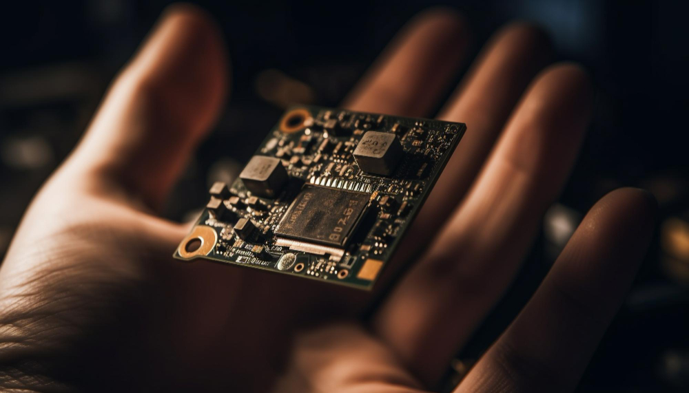
PCB assembly (PCBA) is the process of soldering electronic components onto a bare printed circuit board to produce a functional electronic assembly. While this sounds straightforward, the process encompasses multiple distinct technologies, each suited to different component types, board complexities, and production volumes.
The three primary assembly processes are:
Surface Mount Technology (SMT)
Components are placed directly onto pads on the surface of the PCB and soldered using a reflow oven. SMT supports the smallest component packages: 0201, 01005, QFN, BGA, and LGA and is the dominant process for modern high-density boards. SMT lines are largely automated, and line speed, placement accuracy, and oven profile management are the key differentiators between EMS providers.
Through-Hole Technology (THT)
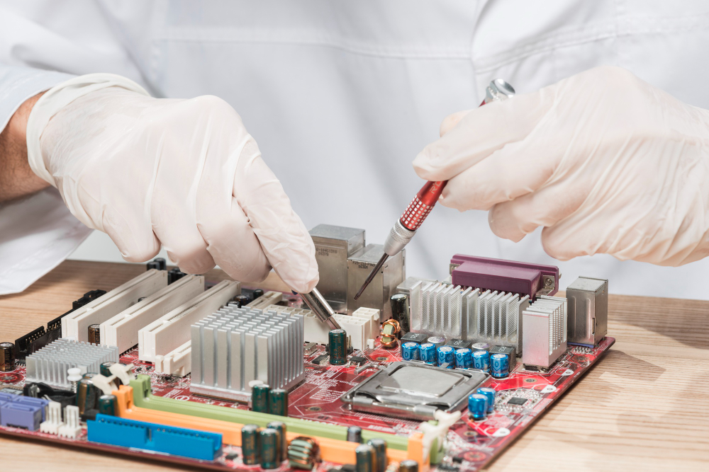
Component leads are inserted through drilled holes in the PCB and soldered on the opposite side, either via wave soldering or selective soldering. THT is used for components that require mechanical strength connectors, transformers, large capacitors, and certain power components. Many modern boards require both SMT and THT, making mixed-technology capability an important selection criterion.
Mixed Technology Assembly
The majority of industrial, automotive, and telecom PCBs require a combination of SMT and THT processes, often with multiple reflow and wave passes. Managing the thermal budget across passes ensuring previously soldered joints aren’t reflowed or disturbed requires both process engineering expertise and tightly controlled equipment. Choosing an EMS partner in Ahmedabad that has all three capabilities under one roof eliminates the risk of sub-contracting, split accountability, and logistics delays between vendors.
The Equipment Stack: What to look lor in an Ahmedabad PCB Assembly facility
Equipment capability is the most objective way to evaluate an EMS partner before visiting their facility. Here is what a capable PCB assembly operation should have and why each piece matters.
Solder Paste Inspection (SPI)
SPI machines measure the volume, area, height, and position of solder paste deposits on PCB pads before components are placed. Poor solder paste deposition is the root cause of a significant proportion of soldering defects: bridging, insufficient solder, and opens. An EMS partner running SPI after the stencil printer catches paste defects before they become component-level defects, dramatically reducing rework costs.
Ask any prospective partner: “Do you run 100% SPI on every board?” If the answer is no, or “only on complex boards,” that is a process risk.
Automated Optical Inspection (AOI)
AOI machines use cameras and image processing algorithms to inspect placed and soldered components against a golden reference. AOI catches missing components, wrong components, reversed polarity, tombstoning, bridging, and insufficient solder. A capable facility runs AOI at two stages: post-placement (to catch placement errors before reflow) and post-reflow (to catch soldering defects).
X-Ray Inspection
X-ray inspection is non-negotiable for boards containing Ball Grid Array (BGA), QFN, or other bottom-terminated components where solder joints are hidden beneath the package body. 2D X-ray is the minimum; 3D CT X-ray provides cross-sectional views and is required for complex BGA void analysis and rework verification.
If your product contains any BGA components and your EMS partner does not have X-ray capability, they cannot verify solder joint integrity. This is a hard qualification gate.
Pick-and-Place Machine Accuracy
Modern SMT pick-and-place machines are rated by placement accuracy (typically ±25–50 microns at 3 sigma for high-end machines) and component range (minimum component size). For boards containing 0201 or 01005 passives, or fine-pitch ICs below 0.4mm pitch, the pick-and-place machine must be rated for those tolerances. Always ask for the machine make, model, and the smallest component currently in production, not just the machine specification sheet.
Reflow Oven Profile Management
A reflow oven’s temperature profile the ramp, soak, peak, and cooling rates, must be engineered to the specific solder paste and board characteristics. Under-temperature reflow causes cold joints; over-temperature causes component damage, PCB delamination, and intermetallic compound growth that weakens joints over time. A professional EMS partner maintains a profile library for each product and validates profiles against the solder paste manufacturer’s process window.
Quality Standards: IPC Certification and what it actually means
The IPC (Institute for Printed Circuits) publishes the globally accepted standards for PCB assembly quality. The two most relevant for PCBA buyers are:
IPC-A-610: Acceptability of electronic assemblies
This is the definitive reference for PCBA inspection criteria. It defines three classes of acceptance:
- Class 1 – General Electronics: Consumer products where cosmetic defects are acceptable provided function is not impaired.
- Class 2 – Dedicated Service Electronics: Industrial, commercial, and communications products where extended performance life is required.
- Class 3 – High Reliability: Aerospace, medical, military, and life-critical applications where failure is not an option.
When evaluating an EMS partner, specify which IPC class your product requires. An EMS company building to Class 1 criteria is not equipped procedurally or culturally to build a Class 3 product, regardless of their equipment.
IPC-7711/7721: Rework and repair
Governs the processes for reworking and repairing PCBA defects. An EMS partner should follow this standard for all rework, ad-hoc or process-driven rework that doesn’t follow documented procedures is a reliability risk.
Always ask to see the IPC certifications of the operators and inspectors, not just the company. IPC-A-610 Certified Inspection Specialists (CIS) and Certified IPC Trainers (CIT) are the individual-level credentials that demonstrate real process discipline.
Prototyping vs Volume production: Different requirements, different partners

One of the most common mistakes OEMs make when selecting a PCB assembly partner in Ahmedabad is choosing a partner optimised for volume production when they need rapid prototyping or vice versa.
Rapid prototyping requirements
- Fast NPI (New Product Introduction) turnaround, ideally 5–10 working days from Gerber and BOM to assembled boards
- Flexibility to handle low quantities (5–50 boards) without minimum order quantity penalties
- Engineering engagement, the ability to flag BOM issues, component substitutions, and DFM concerns before assembly starts
- Willingness to work with customer-supplied components
Volume production requirements
- Consistent cycle times and OEE (Overall Equipment Effectiveness) on the SMT line
- Statistical Process Control (SPC) data for key process parameters
- Component supply chain management: The ability to source, inspect, and manage a full BOM
- Established ECO (Engineering Change Order) handling process
- Packaging and labelling to customer specifications
The best EMS partners in Ahmedabad handle both with a dedicated NPI process that transitions products from prototype to volume production using the same tooling, programs, and quality records. This continuity eliminates the handoff risk that comes with using separate vendors for prototyping and production.
DFM: The Conversation Your EMS Partner Should Be Having With You
Design for Manufacturability (DFM) review is the process of analysing a PCB design before manufacturing to identify features that will cause yield losses, assembly difficulties, or reliability problems. A capable EMS partner conducts a formal DFM review on every new product and documents findings for the customer.
Common DFM issues that a thorough review catches:
Insufficient Component Clearance
Components placed too close together prevent AOI camera access, complicate rework, and can cause shadowing during wave soldering.
Thermal Imbalance on Pads
Asymmetric copper pour around component pads causes uneven heat distribution during reflow, leading to tombstoning of small passives.
Testpoint Accessibility
Products that require In-Circuit Testing (ICT) or Flying Probe Testing need accessible test points on the PCB. Missing or inaccessible test points discovered after PCB fabrication require a board re-spin, expensive and time-consuming.
Stencil Aperture Design
Pad geometry and stencil aperture ratio directly affect solder paste release. Apertures with an area ratio below 0.66 will have inconsistent paste release, leading to solder defects on fine-pitch components.
If your prospective EMS partner in Ahmedabad does not offer a formal, written DFM review as part of their NPI process, you are carrying design risk that will surface as yield loss in production.
Supply chain and component traceability
For regulated industries, medical devices, automotive electronics, defence, and industrial safety systems, full component traceability from manufacturer to assembled board is a non-negotiable requirement. This means:
- Maintaining Certificates of Conformance (CoC) from component manufacturers or authorised distributors
- Lot code and date code tracking at the component level
- First-In-First-Out (FIFO) inventory management to prevent component aging
- Moisture Sensitive Device (MSD) handling per IPC/JEDEC J-STD-033
- Counterfeit component detection: Visual inspection, X-ray, and electrical testing of components from non-authorised supply sources
A professional EMS partner in Ahmedabad should be able to demonstrate their supply chain policy and provide documented evidence of CoCs for your product’s critical components.
Testing: The final gate before shipment
Assembly without testing is not assembly, it’s gambling. A capable PCB assembly partner in Ahmedabad should offer one or more of the following test methodologies:
In-circuit testing (ICT)
Uses a bed-of-nails fixture to probe test points across the PCB, verifying component placement, orientation, value, and basic functionality. ICT provides high fault coverage but requires a custom fixture (typically 3–6 week lead time) and is most cost-effective at medium to high volumes.
Flying probe testing
A fixtureless alternative to ICT where motorised probes move across the board testing each net individually. Slower than ICT but ideal for prototypes, low volumes, and products with frequent design changes where fixture investment isn’t justified.
Functional testing (FCT)
Tests the assembled board as a complete system applying power, stimulus, and measuring outputs against a specification. FCT is the ultimate gate for shipping confidence but requires customer-supplied test fixtures and test software. A capable EMS partner will work with your engineering team to implement and document your FCT procedure.
Burn-in testing
For high-reliability applications, boards are subjected to elevated temperature and voltage stress over a defined period to precipitate early-life failures before shipment. Burn-in screens out infant mortality failures that would otherwise appear in the field within the first hours of customer use.
Why location in Ahmedabad matters for your supply chain
Choosing a PCB assembly partner in Ahmedabad offers practical supply chain advantages for OEMs based in Gujarat or Western India:
- Proximity to Component Suppliers: GIDC industrial estates across Gujarat, combined with component distributor hubs in Ahmedabad, provide access to passives, connectors, and standard semiconductors with short lead times.
- Logistics Efficiency: For OEMs shipping nationally or exporting through Mundra Port, Ahmedabad-based EMS provides a logistically efficient base with direct road connectivity.
- Competitive Pricing: Ahmedabad offers compelling EMS pricing compared to Bengaluru or Pune without compromising on technical capability, a meaningful cost differential at medium volumes (500–5,000 assemblies per month).
- Engineering Talent Pool: The city’s engineering colleges and established industrial base have produced a local pool of electronics engineers, quality technicians, and production operators with genuine domain experience in PCB assembly.
The 12 questions to ask before selecting a PCB Assembly partner in Ahmedabad
Use this checklist when evaluating any EMS partner:
- What SMT equipment do you run, and what is the smallest component you currently place in production?
- Do you run 100% SPI after paste printing on every job?
- What AOI equipment do you use, and at which stages of the process?
- Do you have X-ray capability? What is the make and model?
- What IPC standard do you build to Class 1, 2, or 3?
- Are your operators and inspectors IPC-A-610 certified?
- What is your standard NPI process and typical prototype turnaround time?
- Do you offer a formal DFM review, and is it documented?
- How do you handle component traceability and Certificates of Conformance?
- What testing do you offer: ICT, Flying Probe, FCT, Burn-In?
- Can you provide process SPC data for key parameters?
- What is your documented rework process, and do you follow IPC-7711/7721?
An EMS partner who answers all twelve questions clearly with documentation to back them up, is a partner worth engaging seriously.
Conclusion: Precision is not a feature, it’s the foundation
PCB assembly in Ahmedabad has matured significantly. The question for OEMs is no longer whether capable partners exist in the city, they do but how to identify the ones whose process discipline, equipment capability, and quality culture match the demands of your product.
The right EMS partner is not just a contract manufacturer. They are an extension of your engineering and quality team, one who catches problems before they become field failures, who engages with your design proactively, and who scales with your product as it moves from prototype to volume production.
At Alica Technologies, we have built our PCB assembly operation in Ahmedabad around exactly these principles: IPC-recommended SOPs, end-to-end inspection using SPI, AOI, and X-ray, rapid prototyping capability, and a technical team that engages at the DFM stage, not after the first build failure.
If you’re evaluating PCB assembly partners for your next project, we’d welcome a technical conversation.
Get a Quote |
View Our Services |
Call us: +91 97271 78787
Alica Technologies LLP is an Electronics Manufacturing Services (EMS) company based in Ahmedabad, Gujarat, specialising in PCB assembly, SMT & THT production, AOI & X-ray inspection, and turnkey electronic manufacturing for OEMs across India.